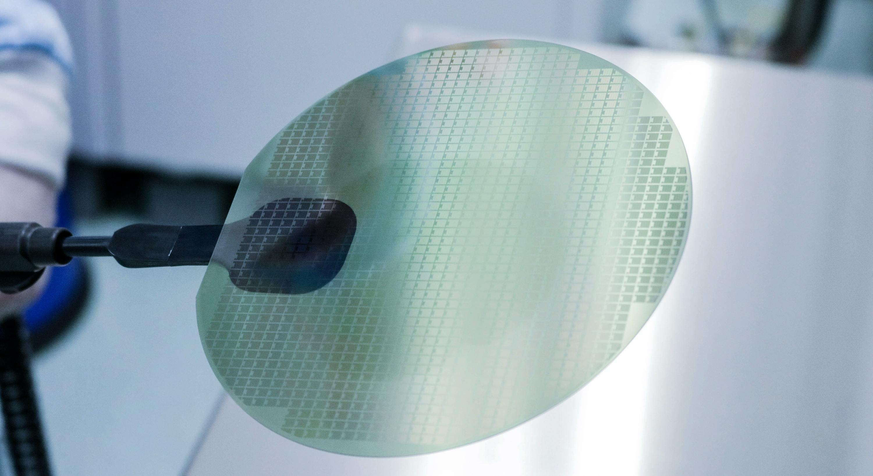
SiC Power MOSFETs

Whether for fast charging of electric vehicles and smartphones, loss-free voltage conversion in solar systems, or uninterruptible power supply in industry or medical technology, silicon carbide (SiC) is particularly well suited for applications in power electronics. The permanently increasing demands on performance, efficiency and speed have reached areas that silicon can no longer cope with as substrate. SiC MOSFETs, for example, have up to 90% lower switching losses compared with silicon-based IGBTs.
Although SiC compound semiconductors are more expensive to manufacture, these devices have distinct advantages. They allow switching frequencies that make it possible to reduce the size and weight of passive components. By using lighter, more compact and passively air-cooled heat sinks, more efficient systems can be realized without separate thermal management with liquid or fan. Particularly in view of the progressive expansion of renewable energy sources and the growing electromobility market, the use of SiC transistors is expected to increase.
What makes a SiC Power MOSFET?
Wide band gap
Silicon carbide has a larger band gap than silicon. Thus, electrons require considerably more energy to reach the conduction band. This results in an electric field strength of silicon carbide that is about 10 times greater than silicon, which in turn means that SiC allows 10 times higher voltages without system failure. Conversely, a larger breakdown field strength means that a much thinner layer topology with lower conduction resistance than silicon is required. The higher carrier mobility and thinner layer topology (space charge region) allow shorter switching times and reduced energy loss. The significantly higher thermal conductivity of SiC also enables higher current densities, so that a SiC device can be much smaller than a corresponding component made of silicon. Due to the higher switching frequencies at system level, the impedances (coils & capacitors) are reduced. This reduces the volume and weight of systems by approximately 75%, which is a major additional advantage, especially for use in electric cars.
In summary, for the same chip size and voltage, a SiC MOSFET has up to 90% lower ON resistance and less dynamic switching losses, which result in electrical power loss that is dissipated in the form of heat.
New structures and improved gate oxides
Among the multiple design concepts for active SiC power devices that have appeared in recent years, the voltage-controlled (normally off!) MOSFET has emerged as the most common solution. This design has also been further improved by using non-planar structures and significantly improving the extrinsic failure rate of the gate oxide.
Planar channels exhibit relatively weak conductivity. Thus, the components must be operated with high field strengths due to their comparatively thin gate oxide layer. However, this increased performance has a negative impact on reliability, as the risk of system failure increases due to the continuous stress on the gate oxide. Trench gate concepts offer a compromise for this, as they provide significantly higher channel conductivity compared to planar channels and require significantly less of the expensive SiC substrate area, reducing device size and cost.
The interface between gate oxide and SiC plays a decisive role in the performance of the SiC MOSFET. Therefore, manufacturers pay particular attention to its improvement and further development. Post-oxidation annealing (POA) and passivation of the SiC interface are applied for this purpose, for example.
How does centrotherm process technology contribute?
For SiC MOSFET production, we have established ourselves as the global technology leader for high-temperature annealing and oxidation processes. In addition, we provide further thermal processes such as oxidation, annealing, diffusion and LPCVD in the atmospheric and low-pressure range. Our strong market presence in SiC also gives us access to upstream value-added stages such as ingot, boule and wafer manufacturing for which we offer annealing processes for healing crystal defects and dislocations.
